What are the differences between STM32V8 chips used in Starlink’s laser communication systems compared to the hobby STM32s?
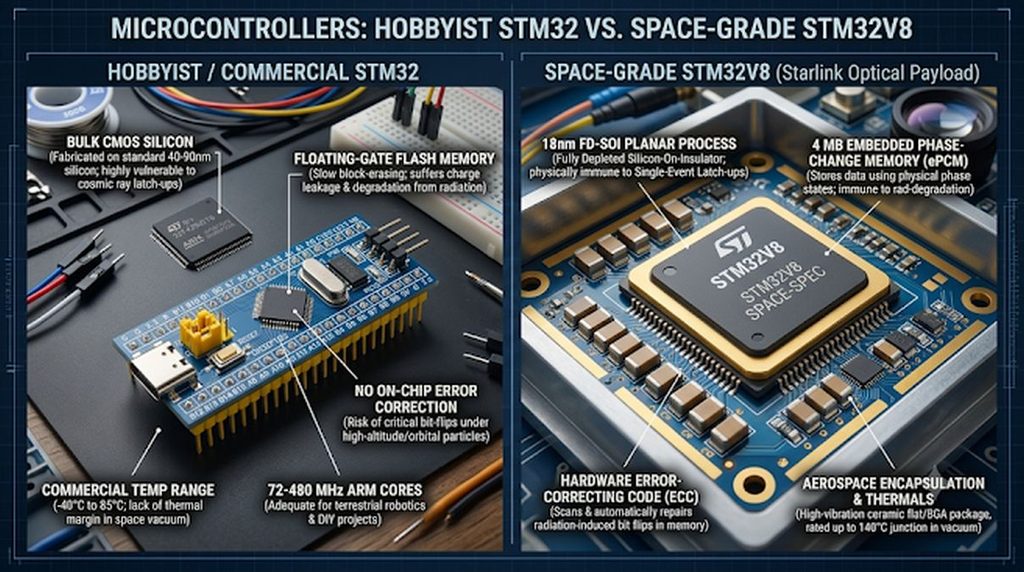
While the STM32V8—selected by SpaceX for Starlink’s mini inter-satellite laser communication terminals—shares the same STM32Cube software ecosystem as hobbyist boards, its underlying silicon, memory physics, and compute architecture are built for Low Earth Orbit rather than the workbench.
In Starlink’s optical terminals (which link satellites across up to 4,000 km at speeds up to 25 Gbps), the STM32V8 handles real-time beam pointing, fast-steering mirror control loops, and link management under constant radiation exposure.
1. Silicon Process & Radiation Tolerance (18 nm FD-SOI vs. Bulk CMOS)
- STM32V8: Built on an 18 nm FD-SOI (Fully Depleted Silicon-On-Insulator) planar process co-manufactured at ST’s Crolles fab in France (with Samsung Foundry adding U.S. capacity in Austin). An ultra-thin buried oxide (BOX) layer isolates the transistor channel from the underlying silicon wafer. In orbit, this eliminates the parasitic pathways that cause destructive Single-Event Latch-ups (SELs) and drastically shrinks the charge-collection volume vulnerable to Single-Event Upsets (SEUs) from cosmic rays and trapped protons.
- Hobby STM32s (F1, F4, G4, H7): Fabricated on older 90 nm down to 40 nm bulk CMOS processes. Because transistors sit directly in a shared silicon substrate, high-energy particles in space can easily flip register bits or trigger latch-up currents without heavy external shielding.
2. Non-Volatile Memory (Embedded PCM vs. Floating-Gate Flash)
- STM32V8: Replaces conventional Flash with up to 4 MB of embedded Phase-Change Memory (ePCM). Instead of trapping electrons behind an insulating gate oxide—which gradually leaks charge under cumulative orbital radiation—PCM stores
1s and0s by switching a chalcogenide alloy between amorphous (high-resistance) and crystalline (low-resistance) physical states. It also writes directly without slow block-erase cycles and endures up to 100,000 write cycles. - Hobby STM32s: Use standard embedded NOR Flash (typically 64 KB to 2 MB), which degrades under Total Ionizing Dose (TID) radiation and requires high-voltage charge pumps to erase blocks before reprogramming.
3. CPU Architecture & Real-Time DSP Math
- STM32V8: Powered by an Arm Cortex-M85 core running up to 800 MHz (~5,072 CoreMark), paired with Arm Helium (M-Profile Vector Extension / MVE) for 128-bit SIMD vector and floating-point math, plus dedicated CORDIC (trigonometric) and FMAC (filter math) accelerators. That deterministic vector math allows a single MCU to compute sub-microradian optical tracking corrections in microseconds.
- Hobby STM32s: Classic maker chips like the STM32F103 (“Blue Pill”) run a 72 MHz Cortex-M3 (~177 CoreMark), STM32F4 chips (“Black Pill”) run a 100–180 MHz Cortex-M4 (~608 CoreMark), and high-end hobbyist STM32H7 chips run a 480–600 MHz Cortex-M7 (~3,347 CoreMark). Even against an STM32H7, the STM32V8 delivers roughly 3.5x to 6x higher DSP and edge-AI throughput.
4. Error Correction, Thermal Limits & Peripherals
- STM32V8: Integrates 1.5 MB system SRAM and up to 512 KB Tightly Coupled Memory (TCM) protected by Error-Correcting Code (ECC) across both ePCM and critical RAM banks to detect and repair single-bit radiation flips on the fly. It’s rated up to a 140 °C junction temperature (important in vacuum where heat only leaves via conduction and radiation) and includes 1 Gbps Ethernet with Time-Sensitive Networking (TSN), I3C, Octo/Hexa-SPI, and PSA Level 3 / SESIP3 hardware cryptography.
- Hobby STM32s: Mostly lack RAM/Flash ECC, are rated to 85 °C, and top out at USB FS/HS, CAN, or standard 10/100 Ethernet.
Related Posts


About The Author
